Tesla Deepens AI Chip Roadmap: Samsung’s 2nm Process to Power Next-Gen AI6, Boosting Foundry Business
Samsung Electronics is poised to significantly expand its involvement in Tesla’s advanced AI chip production. This follows Tesla’s successful completion of the design for its next-generation AI5 processor, a crucial development that could rejuvenate Samsung’s foundry division, which has faced recent challenges.
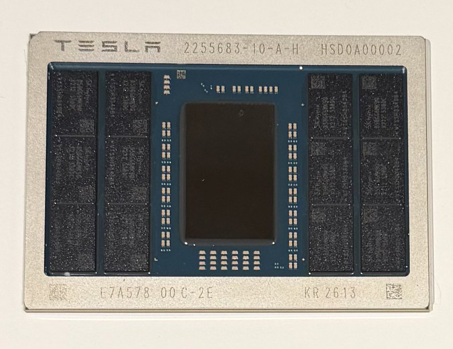
Tesla CEO Elon Musk confirmed on Wednesday that the company’s dedicated AI chip team had “taped out” the AI5 processor. This pivotal step signifies the finalization of the chip design, making it ready for production by manufacturing partners.
“Congrats to the @Tesla_AI chip design team on taping out AI5! AI6, Dojo3 & other exciting chips in work,” Musk posted on his X account, hinting at an ambitious future for Tesla’s in-house chip development.
In a subsequent post, Musk further revealed that both Samsung and TSMC are lined up to support the production of these groundbreaking chips, predicting that they will become “one of most produced AI chips ever.”
The AI5 chip is slated to become the foundational processor for Tesla’s fifth-generation full self-driving (FSD) hardware, known as HW 5.0. Furthermore, it is anticipated to drive the company’s advanced humanoid robot initiatives, positioning it centrally within Tesla’s expansive AI strategy.
Tesla’s adoption of a “multi-foundry” strategy, leveraging the world’s leading contract chip manufacturers, aims to bolster capacity and mitigate supply chain vulnerabilities in the intense global competition for advanced-node chips.

Samsung has a proven track record, having previously supplied earlier-generation AI4 chips. Last year, the Korean tech giant further solidified its partnership by securing a significant contract, estimated at approximately 23 trillion won ($15.6 billion) through 2033, to produce Tesla’s cutting-edge AI6 processors.
Offering further insights into Tesla’s extensive chip roadmap on Thursday, Musk stated that the AI6 will be manufactured utilizing Samsung’s advanced 2nm process at its Texas fabrication plant. This is expected to deliver nearly double the performance of AI5 within the same die footprint. An even more powerful iteration, the AI6.5, is slated for production on a 2nm node by TSMC in Arizona, promising additional performance enhancements.
While specific financial terms for the AI5 volumes remain undisclosed, their inclusion significantly strengthens the strategic alliance between Samsung and Tesla. This collaboration offers Samsung a prominent platform to validate its leading-edge process technology in a high-demand application.
Production is anticipated to be distributed across various facilities capable of handling 2- to 3-nanometer nodes. Samsung is expected to utilize its cutting-edge Taylor fab in Texas, complementing its established capacity in Pyeongtaek, Korea, where AI4 chips were previously manufactured.
These substantial Tesla orders arrive at a pivotal moment for Samsung. Its foundry unit has recently reported quarterly losses nearing 1 trillion won, largely due to diminished order volumes and fierce competition from industry leader TSMC. Attracting high-profile AI customers like Tesla is considered vital for reversing these financial challenges and bolstering its market position.
Samsung had previously indicated it is engaged in active discussions with key clients across the US and China. The company projects a significant surge, over 130 percent this year, in orders for its 2nm chips specifically designed for high-performance computing (HPC) and advanced AI applications.
Beyond its advancements in automotive chips, Samsung is actively broadening its advanced-node production pipeline. The company has secured the manufacturing of DeepX’s second-generation AI processor using its 2nm process, with mass production anticipated in 2027. Concurrently, Samsung is producing its proprietary Exynos 2600 mobile processor for smartphones, employing gate-all-around (GAA) architecture – a critical trial for both its chip design and fabrication capabilities.
Furthermore, Samsung’s foundry division is forging closer ties with its memory business. Company executives have revealed that the base die for the next-generation high bandwidth memory (HBM5) is under development on a 2nm process, representing a significant leap from the 4nm node utilized in HBM4.