CTO reveals next-gen HBM4 surpasses expectations, as Samsung aims to reclaim AI memory leadership.
Samsung Electronics leveraged Semicon Korea 2026 to emphasize its advancements in next-generation artificial intelligence (AI) memory. The tech giant highlighted positive customer feedback on its sixth-generation high bandwidth memory (HBM), HBM4, and introduced an expanded roadmap for advanced packaging solutions.
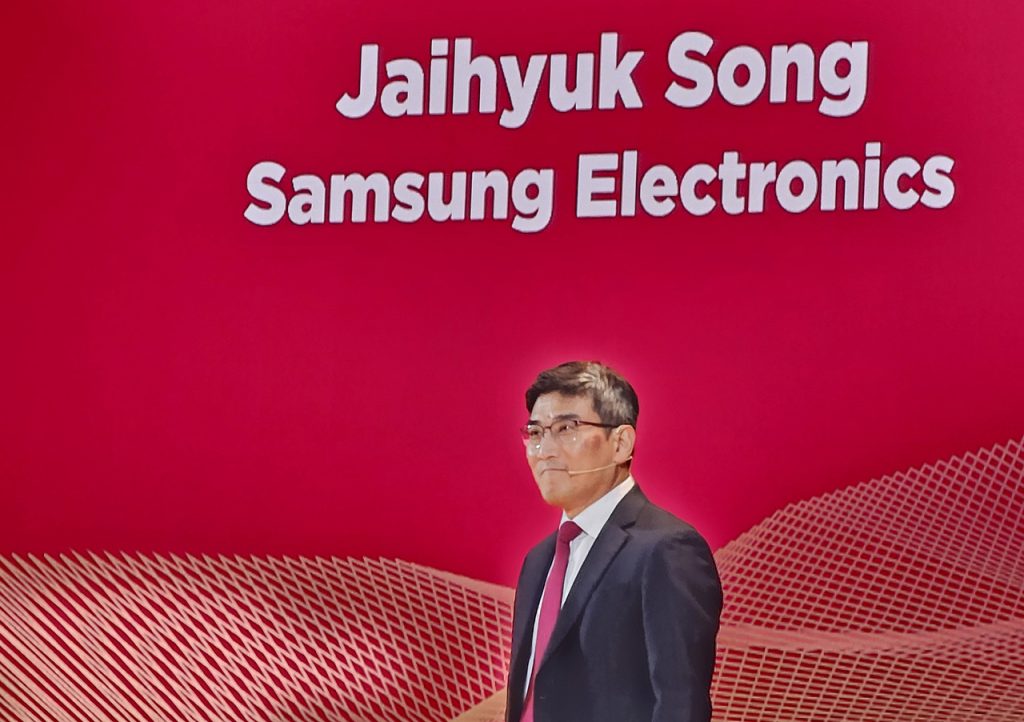
Song Jai-hyuk, Chief Technology Officer of Samsung’s device solutions division, stated that the response to HBM4 has been “very satisfactory,” and that the company is gearing up for mass production shipments later this month.
Samsung and SK hynix are anticipated to be key suppliers of HBM4 for Nvidia’s upcoming AI accelerator platform, Vera Rubin. These new memory chips boast data transfer speeds of 11.7 gigabits per second (Gbps), exceeding Nvidia’s requirement of 11 Gbps and setting a new performance standard in the industry.
According to Song, Samsung’s vertically integrated structure – encompassing memory, foundry, and advanced packaging capabilities – enables the company to swiftly adapt to the evolving demands of the AI market. He further added that future generations, including HBM4E and HBM5, are already under development.
During his keynote address, Song detailed Samsung’s comprehensive memory strategy, which centers around custom HBM, vertically integrated zHBM, and Hybrid Copper Bonding technology.
Custom HBM is engineered to offload specific processing tasks from the graphics processing unit (GPU) to the base die within the HBM stack, thereby improving performance efficiency. zHBM, on the other hand, vertically integrates memory with compute chips, such as central processing units (CPUs) and GPUs, through 3D stacking, with the goal of enhancing bandwidth and minimizing power consumption.
To facilitate these advanced architectures, Samsung intends to implement Hybrid Copper Bonding, a technology that directly bonds chips without the use of microbumps. This approach allows for thinner dies, shorter interconnect distances, and accelerated data transfer speeds, highlighting the increasing significance of advanced packaging in optimizing AI chip performance.
Samsung’s presentation coincided with industry analysts emphasizing that the growth of AI infrastructure is becoming increasingly reliant on advancements in memory and packaging technologies, rather than solely on wafer capacity.
Clark Tseng, Senior Director of Market Intelligence at Semi, explained during a briefing that record capital expenditure in the AI sector does not automatically translate into readily available supply.
“We are seeing record levels of capital investment, but spending alone does not resolve bottlenecks,” Tseng said. “The real constraint is shifting from wafer starts to yield, advanced packaging and qualification timelines.”
Semi reports that South Korea’s chip exports reached $173.4 billion in 2025, a 22.2 percent increase compared to the previous year, with December marking a monthly peak of $20.7 billion. Exports to Taiwan experienced a significant surge of 64.8 percent, reflecting a deeper level of integration into the AI accelerator supply chain.
Global semiconductor revenue and AI-related capital expenditure are both projected to surpass $1 trillion by 2027, according to Tseng. Fab capacity is expected to grow from 25 million wafers per month to approximately 45 million by 2030, while South Korea’s annual fab investment is forecasted to reach around $40 billion between 2026 and 2028.
Tseng emphasized that memory and advanced packaging have become system-level constraints in the development of AI infrastructure.
“Memory and packaging are no longer supporting roles,” he stated. “They are now critical to how fast AI infrastructure can scale.”
Lee Sei-cheol, Head of Citi Korea Research, suggested that the next phase of AI demand may gradually transition from centralized cloud systems to more distributed, on-device AI applications. He also noted that back-end process technologies, such as hybrid bonding, are gaining strategic importance alongside front-end wafer fabrication.
Semicon Korea 2026 commenced in Seoul with a record number of preregistered participants. The three-day event is expected to attract over 75,000 visitors and feature 550 exhibitors and more than 200 speakers across 30 conferences.