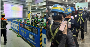
Samsung Electronics is reportedly in advanced discussions to manufacture a crucial component for Google’s next-generation artificial intelligence chips. This potential agreement could significantly bolster Samsung’s position in the evolving semiconductor supply chain, as industry leaders like Taiwan Semiconductor Manufacturing Co. (TSMC) face unprecedented capacity constraints amidst soaring AI demand.
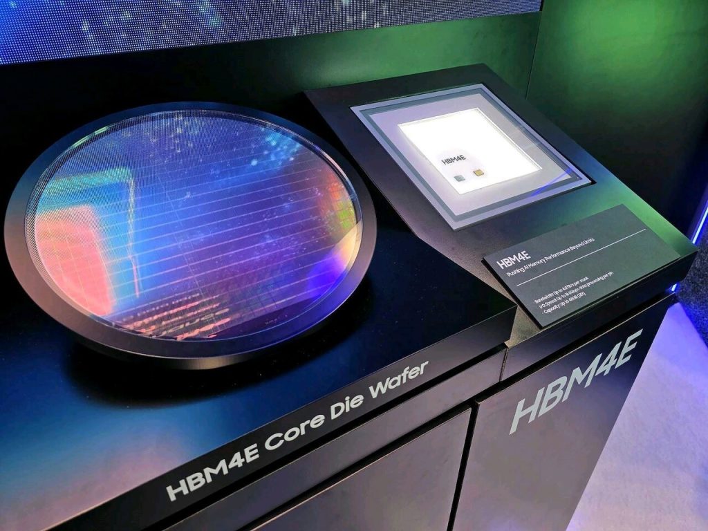
Specifically, Google is exploring the utilization of Samsung’s cutting-edge 2-nanometer process technology for the production of a critical memory input-output (I/O) die. This component is destined for Google’s 10th-generation Tensor Processing Unit (TPU), an advanced in-house chip powering Google’s extensive cloud data centers. Codenamed “Icefish,” this groundbreaking AI chip, as reported by The Information, citing project insiders, is anticipated to enter mass production as early as 2028, although its design phase is still ongoing and subject to adjustments.
When approached for comment on these reports, a Samsung Electronics official informed The Korea Herald that the company was unable to confirm the details at this time.
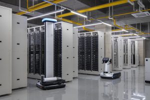
The manufacturing responsibilities for the “Icefish” chip are expected to be strategically divided. TSMC would reportedly handle the production of the advanced computing engine, the most technically demanding segment, utilizing its forthcoming 1.4-nanometer technology. Meanwhile, Samsung is poised to produce the crucial I/O die, which facilitates the vital connection between the processor and high bandwidth memory (HBM). This connection is deemed critical for AI chips, as it ensures a continuous, high-speed data flow essential for maintaining optimal core utilization. While the specific rationale for assigning this particular task to Samsung wasn’t explicitly detailed in the original reporting, industry observers highlight Samsung’s unparalleled expertise as the world’s largest memory manufacturer, making it a logical choice for this memory-intensive component.
These ongoing discussions are indicative of a broader industry trend.
Indeed, TSMC’s most advanced fabrication lines are currently operating at full capacity. CEO C.C. Wei recently informed shareholders that the global chip supply is projected to fall short of escalating AI demand for several years. This capacity crunch is pushing companies to diversify. Concurrently, Google has reportedly placed an order for over 3 million TPUs from Intel, slated for 2028 delivery, and is also collaborating with Taiwan’s MediaTek on the foundational “Icefish” design.
Both Samsung and Google representatives declined to provide official comments to the outlet regarding these developments.
This strategic timing could significantly benefit Samsung, particularly as its foundry unit has actively sought to narrow the market share gap with TSMC since its establishment in 2017. Industry analysts, as reported by Korean media, anticipate Samsung’s contract chipmaking division could return to profitability as early as the third quarter. This would mark its first profit turnaround since experiencing substantial losses in 2022, driven by improved 2nm process yields and an increase in new orders.
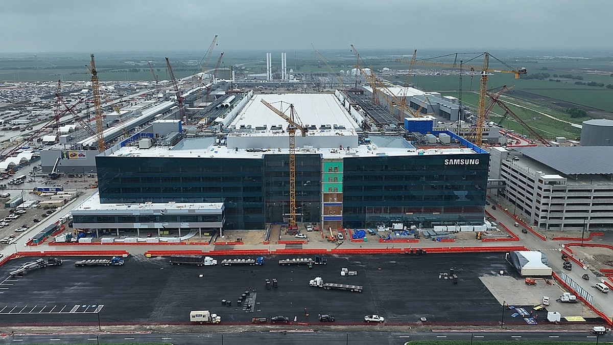
Further solidifying its market position, Samsung secured a significant 22.8 trillion won ($15 billion) long-term contract from Tesla last year for the production of next-generation AI chips. Mass production for this endeavor is slated to commence at Samsung’s new fabrication plant in Taylor, Texas, during the second half of this year. Additionally, Samsung is involved in manufacturing Nvidia’s advanced new language processing unit, underscoring its diverse portfolio.
According to data from Counterpoint Research, TSMC’s dominance in the global pure foundry market expanded to 73 percent in the first quarter, up from 69 percent in late 2024. In contrast, Samsung’s market share experienced a slight decline to approximately 7 percent during the same period, highlighting the competitive landscape.