
Samsung, LG, and SK Target Glass Substrates for Next-Gen AI Chip Packaging Amidst Mass Production Challenges
LG Innotek CEO Moon Hyuk-soo recently encapsulated Korea’s strategic focus on the next evolution of AI hardware. He noted that while the development of advanced **glass substrates** for **AI chip packaging** is largely complete, significant challenges, or “homework problems,” persist before **mass production** can be realized.
Overcoming these hurdles to commercialize **glass substrates** represents a multi-billion dollar opportunity within the **semiconductor industry**.
This year’s most impactful AI-related market activity in Korea hasn’t been centered on chips themselves, but rather on the companies supplying critical surrounding components. **Samsung Electro-Mechanics** and **LG Innotek** have seen their stock values surge in 2026. This growth is attributed to acute shortages in **high-end package substrates** and, for Samsung Electro-Mechanics, the specialized capacitors essential for stable power delivery to chips, granting these firms unexpected pricing advantages.
Recognizing the cascading investment in AI technology, investors are now keenly observing the next major innovation. This emerging technology, more fundamental than even advanced capacitors, involves engineered **glass substrates** designed to underpin the **AI chips** themselves.
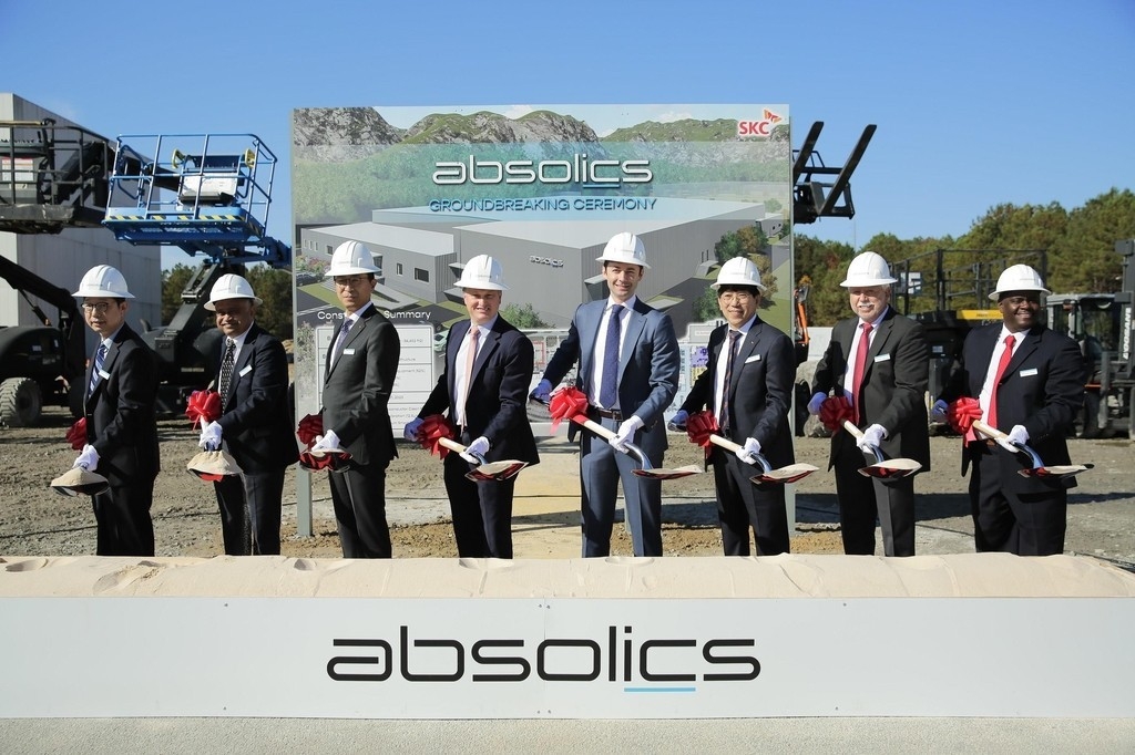
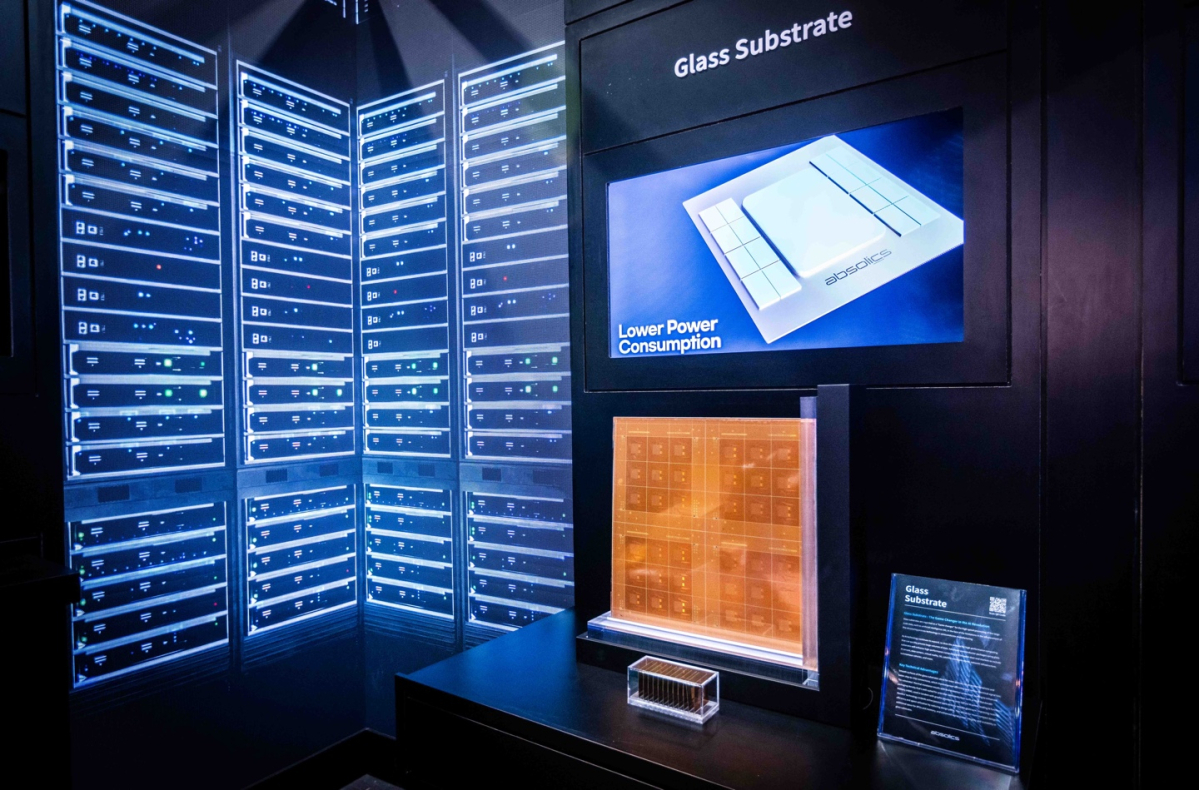
The most ambitious play in this emerging sector isn’t from current market leaders like Samsung or LG. Instead, it comes from **SKC**, a mid-sized chemicals conglomerate that has strategically divested most of its other assets to aggressively pursue **glass substrate technology**. Its U.S. subsidiary, **Absolics**, established a dedicated facility in Covington, Georgia, with the singular goal of becoming the world’s first company to achieve **mass production of glass substrates** for semiconductors.
However, the industry continues to await this critical breakthrough in **glass substrate mass production**.
Glass Substrates: The Essential Platform for High-Performance Chips
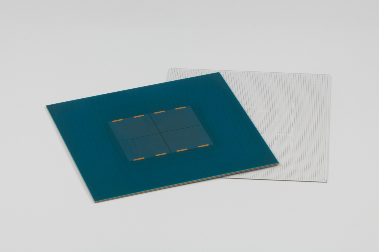
At its core, the concept is straightforward: every **advanced semiconductor chip** relies on a foundational platform. This platform facilitates the intricate connection between the chip’s microscopic wiring and the broader circuitry of the underlying printed circuit board. Currently, these essential platforms are constructed from multi-layered plastic resins, a technology that has served its purpose effectively.
Yet, as **AI accelerators** become increasingly powerful, larger, and generate more heat, traditional plastic substrates present significant limitations. Similar to how wood can warp in humidity, plastic can bend under thermal stress, leading to distortion and degradation of the critical electrical signals it is designed to transmit.
In contrast, **glass substrates** offer superior material properties. Glass maintains exceptional flatness, minimizing signal loss and enabling more efficient power and data transmission within a denser **chip package**. The fundamental argument is that by replacing the plastic base with glass, a critical bottleneck in the evolution of **AI hardware** can be effectively addressed.
However, the primary obstacle lies within the **manufacturing process** itself.
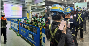
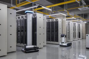
Cha Yong-ho, an analyst with LS Securities who visited the **Absolics** production line in 2024, highlighted the intricate nature of **glass substrate manufacturing**, noting it integrates expertise from three distinct industries: approximately 50% from traditional substrate production, 30% from display technology, and 20% from semiconductor processes. He estimates the production involves around 190 meticulous steps before final inspection, all while handling a material inherently prone to shattering. Even a minute crack during early stages can lead to complete component failure during subsequent testing or **packaging**.
For this reason, Cha views **glass substrates** not as a distinct innovation but as a natural evolution within the current surge in **AI component development**. He posits that **glass substrates** represent “the next chapter of FC-BGA technology, rather than an isolated trend.”
Unraveling the Delays in Glass Substrate Commercialization
The difficulty extends beyond merely drilling microscopic holes through the glass. The process demands intricate plating, precise layer stacking, accurate panel cutting, and thorough inspection of the final **semiconductor component**—all without compromising its delicate integrity.
Clark Tseng, Senior Director of Market Intelligence at SEMI, the leading global chip industry association, characterizes the current market for **glass substrates** as an “exploratory phase.” He views **glass core substrates** as “one possible solution” for future **high-end chip packages**, rather than an established replacement for existing materials. Tseng further predicts that “meaningful volume” of **glass substrate mass production** is improbable before approximately 2028.
Concurrently, China is actively advancing its own capabilities in **glass substrates**, leveraging expertise from its display and PCB industries. BOE has publicly announced the completion of a pilot line for large-area **glass substrates**, while companies like Visionox and AKM Meadville are also making strategic entries into this specialized domain.
A Korean materials industry insider noted that Chinese firms appear to be adopting an accelerated, integrated approach to **glass substrate manufacturing**, potentially hastening their market entry.
Despite industry skepticism, **SKC** maintains that its subsidiary **Absolics** is closer to achieving breakthroughs than the market perceives. Reports indicate that a sample **glass substrate** has been sent to a U.S. chip customer for crucial reliability testing. The company has suggested that successful qualification could enable preparations for production to commence this year.
The challenge, however, lies in **SKC’s** repeated optimistic timelines in the past. Initial expectations for commercial output were set for 2024, then postponed to 2025, and subsequently to customer approval in early 2026. In its latest regulatory filing, the company transparently admitted it could no longer provide a definitive **mass production date**.
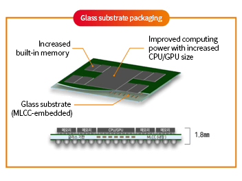
The filing also underscored a more profound technical hurdle. **Absolics’** flagship design, which Im So-jung of Eugene Investment & Securities terms “subtraction and hiding,” is a complex yet highly valuable innovation. This technique involves embedding capacitors and other miniature components directly within the **glass substrate**, thereby shrinking the overall **chip package** and creating more surface area for the primary computing chips. According to **Absolics**, this advanced approach could reduce package height from 3.9 millimeters to a mere 1.8 millimeters. Ironically, this highly ambitious version of **glass substrate technology** is precisely the one experiencing persistent delays.
SKC’s High-Stakes Bet on Glass Substrates: A Pivotal Strategic Move
The ultimate question of whether **glass substrates** will achieve **mass production volume** remains unanswered. However, the varying strategic investments of key industry players are becoming clear. **Samsung Electro-Mechanics** and **LG Innotek** are adopting a more cautious approach. Given their established customer base from the recent **AI components** boom, they can position **glass substrate technology** as a strategic future enhancement rather than an immediate imperative for survival. Samsung, for instance, initiated a **glass-core substrate** joint venture with Japan’s Sumitomo Chemical late last year, targeting significant production volumes beyond 2027.
Similarly, **LG Innotek** has indicated 2028 as its target for **glass substrate commercialization**.
In stark contrast, **SKC** lacks a similar fallback position. Over the past several years, the company has undertaken a comprehensive corporate restructuring, systematically divesting its chemicals, film, and other business units to entirely refocus its operations around **glass substrate technology**. This spring, **SKC** further reinforced its commitment by raising an additional 1.17 trillion won (approximately $840 million) from shareholders, with roughly half of these funds earmarked for **Absolics**. Consequently, the future trajectory of **glass substrates** is now inextricably linked to the fate of **SKC**.
mjh