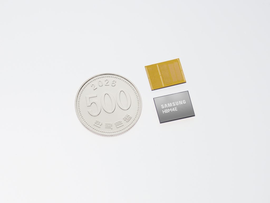
Samsung Leads HBM4E Innovation with First 12-Layer Chip Samples, Intensifying AI Memory Race
Samsung Electronics announced Friday it has commenced supplying samples of the world’s inaugural 12-layer HBM4E chip to key customers, underscoring its strategic initiative to expand its leadership in the booming artificial intelligence (AI) memory market.
This significant launch follows closely, just three months after Samsung initiated mass shipments of its HBM4 predecessors. Memory manufacturers are rapidly accelerating the development of next-generation high-bandwidth memory chips to meet the escalating demands from advanced AI models and hyperscale data centers globally.
The 12-layer HBM4E from Samsung boasts impressive per-pin speeds ranging from 14 to 16 gigabits per second, representing a performance uplift of over 20 percent compared to its HBM4 predecessor.
Crucially, this advanced chip delivers an extraordinary bandwidth of 3.6 terabytes per second per stack. This formidable capability, as highlighted by the tech giant, is engineered to significantly enhance computing performance for demanding applications such as large language models (LLMs) and other complex AI workloads, which are critical for deep learning and machine intelligence.
Equipped with 48 gigabytes of high-bandwidth memory, the 12-layer HBM4E product offers over 30 percent more capacity than the prior generation. Samsung also disclosed plans to broaden its HBM4E product lineup, anticipating future customer demand and system requirements by introducing 32GB eight-layer and 64GB 16-layer versions.
Powering this innovative solution is Samsung’s cutting-edge 1c DRAM – the company’s sixth-generation 10-nanometer-class DRAM process. Additionally, a sophisticated 4-nanometer logic die, meticulously produced through Samsung’s proprietary foundry technology, is integrated to optimize performance.
Samsung affirmed that the synergistic combination of these advanced DRAM and logic process technologies has significantly enhanced production stability, improved manufacturing yield rates, and accelerated readiness for high-volume mass production, ensuring reliable supply for the AI industry.
Furthermore, Samsung detailed substantial improvements in energy efficiency, boasting a 16 percent reduction, and enhanced thermal resistance characteristics by over 14 percent compared to the previous generation. These gains were achieved through meticulous low-power design strategies and sophisticated package optimization techniques, critical for sustained performance in data centers.
Samsung is strategically poised to commence mass supply of this groundbreaking HBM4E product, aligning precisely with individual customer deployment schedules to ensure seamless integration.
“Building on the successful mass production of our HBM4 offerings, Samsung has once again unequivocally demonstrated its distinct technological leadership and innovation with HBM4E,” stated Hwang Sang-joon, Head of Memory Development at Samsung Electronics. “This reaffirms our commitment to pushing the boundaries of memory technology.”
“Through our unparalleled advanced manufacturing capabilities and strategic, preemptive infrastructure investments, we are dedicated to continuously driving the exponential growth and evolution of the global AI memory market,” he added.
The high-stakes HBM4E market is anticipated to intensify in competition. Industry sources report that crosstown rival SK hynix is also actively preparing to dispatch its own HBM4E samples to customers. While SK hynix initially targeted the second half of the year for shipments, sources suggest this timeline could potentially accelerate if their development trajectory remains on schedule, further highlighting the fierce rivalry in the AI memory space.
yeeun