China’s EUV Prototypes Show Progress, But Face Significant Mass Production Barriers
Amid stringent US-led export controls, China is aggressively pursuing the development of its indigenous extreme ultraviolet (EUV) lithography tools. However, industry experts remain highly skeptical that the nation can transform its early EUV prototypes into viable mass-production systems within the current decade.
Reports indicate China has successfully developed a prototype EUV machine, reportedly through reverse-engineering older equipment from the leading Dutch supplier, ASML. While China harbors ambitions for mass production by 2028, industry observers caution that a lab-level demonstration of an EUV system is significantly different from achieving commercial-scale manufacturing capabilities.
Ahn Jin-ho, a materials science professor at Hanyang University, notes the feasibility of China showcasing a one-off demonstration of a homegrown EUV system. Yet, he strongly asserts, “Developing an EUV system truly capable of high-volume manufacturing within the next decade remains highly improbable.”
Lacking access to cutting-edge EUV lithography technology – essential for etching circuits thousands of times thinner than a human hair – China has largely depended on deep ultraviolet (DUV) tools. This reliance necessitates repeating patterning steps, leading to comparable results but at a significantly higher cost and reduced manufacturing efficiency for advanced semiconductors.
However, DUV technology presents inherent limitations for China’s ambitious chip aspirations. As global leaders like Samsung and TSMC advance towards 2-nanometer chip production, Beijing has initiated a robust, state-backed EUV development program, reportedly attracting former ASML engineers and significantly increasing investment in this critical semiconductor technology.
Ahn Ki-hyun, executive director of the Korea Semiconductor Industry Association, underscores the critical importance of EUV lithography, stating, “Below 7-nanometer nodes, EUV lithography is effectively indispensable for advanced chip manufacturing.” He acknowledges that if China successfully localizes EUV technology, it could fundamentally reshape the global semiconductor landscape, but cautions that such a feat will not materialize overnight.
EUV expert Ahn Jin-ho from Hanyang University, recently honored by the National Academy of Engineering of Korea, expresses strong skepticism regarding China’s ability to achieve a mass-production ready EUV system by its ambitious 2028 target.
Ahn emphasizes the immense difficulty, noting, “Even industry heavyweights such as Nikon and Canon, which historically dominated the lithography market, could not ‘crack’ EUV technology. This is clearly not a technology amenable to a brute-force approach.”
He further elaborated that even for ASML, the world’s sole supplier of EUV systems, development spanned decades and necessitated a tightly integrated global ecosystem. This includes critical contributions such as ultra-precision optics from Carl Zeiss and highly specialized light-source technologies, highlighting the collaborative complexity.
The optics system undeniably constitutes one of the most formidable hurdles in EUV technology, demanding extraordinary precision in both its design and manufacturing. Equally critical for successful chip production is the seamless integration of the broader EUV ecosystem, encompassing components like masks, pellicles, and photoresists, all engineered to function flawlessly with the lithography tool.
Ahn explains, “Achieving this unparalleled level of optimization – from meticulous particle control to expertly managing the intricate hydrogen environments within EUV systems – requires decades of specialized, accumulated know-how and iterative refinement.”
Despite the challenges, China has made strides in advanced chipmaking by employing older lithography tools and ArF immersion techniques. Through repeated patterning steps, the nation claims to achieve near 3-nanometer capabilities, although most of its cutting-edge node production predominantly operates around the 7-nanometer level.
However, this technological workaround incurs substantial financial penalties. Prominent Chinese companies like ChangXin Memory Technologies, Yangtze Memory Technologies, and Semiconductor Manufacturing International Corporation (SMIC) are facing mounting financial pressure, as the extensive use of multiple patterning significantly inflates their chip production expenses.
An industry official highlighted the fundamental economic hurdle: “In semiconductor manufacturing, it is ultimately about cost-effectiveness and profit margins. If multiple exposures are required merely to replicate the efficiency of a single EUV step, the underlying economics become unworkable.”
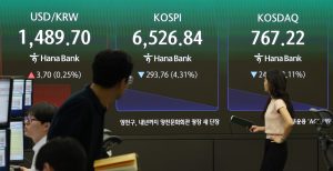
Global Leaders Samsung and SK Hynix Widen EUV Lithography Lead
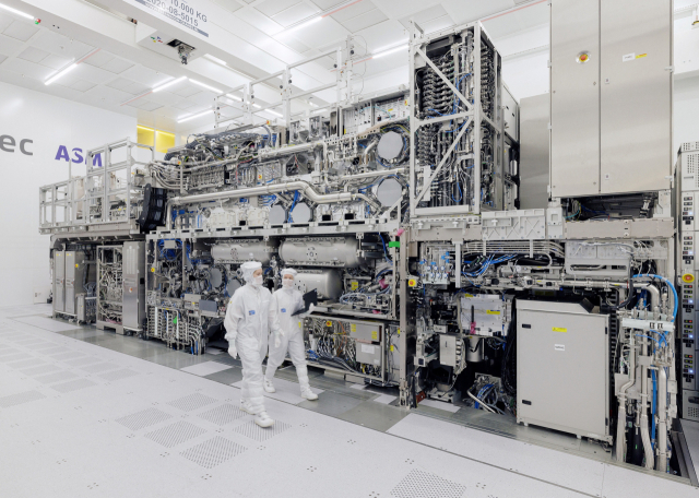
EUV systems, complex machines comprising over 100,000 intricate components, typically command a price tag of $200 million to $300 million per unit. ASML, the sole manufacturer, produces only approximately 70 of these highly specialized semiconductor tools annually.
In a significant strategic move, Samsung recently placed an order for approximately 20 of these scarce EUV machines from ASML. This constitutes a substantial portion of a broader 70-unit lithography equipment purchase for its advanced P5 fab located in Pyeongtaek, Gyeonggi Province. The EUV component of this investment alone is estimated to exceed 10 trillion won ($7.3 billion), highlighting Samsung’s commitment to advanced chip manufacturing.
Similarly, SK Hynix has pledged approximately 11.9 trillion won towards securing EUV tools. These state-of-the-art systems are slated for installation at its Cheongju M15X fab and forthcoming Yongin fabs, with deliveries scheduled through the end of 2026, reinforcing its future semiconductor production capabilities.
Both leading semiconductor companies are strategically deploying these advanced EUV systems to bolster their AI memory production, specifically targeting next-generation high-bandwidth memory (HBM) and other cutting-edge solutions.
However, simply possessing these advanced EUV tools does not solely guarantee a competitive edge in semiconductor fabrication. EUV technology is typically applied only for the most critical layers of chip design, and its overall impact hinges significantly on how effectively it is integrated into the broader, complex semiconductor manufacturing process.
Ahn from Hanyang University further elaborates on the nuances of chip production, stating, “Even when utilizing identical EUV tools, manufacturing outcomes can vary considerably. Factors such as subtle component differences, the precise condition of the equipment, and the crucial experience level of operators all profoundly affect both yield rates and final product quality.”
He concludes by emphasizing that leading chipmakers strategically combine EUV, ArF, and KrF lithography technologies. The astute decisions regarding where and how to deploy each specific technology are pivotal in shaping both overall performance and crucial cost competitiveness in the global semiconductor market.