TSMC Fully Booked at 2nm Through 2028, Opening Door for Samsung
Samsung Electronics is positioning itself to potentially benefit from a constrained supply situation at TSMC. Strong demand for AI chips is pushing the industry leader’s advanced manufacturing capacity to its limits through 2028.
Industry sources indicated on Monday that TSMC has effectively reached full capacity for the coming years. Orders for its leading-edge 2-nanometer process are pouring in from major clients like Nvidia, AMD, Qualcomm, and Apple. Reports suggest even its planned Arizona fabrication plant, slated for mass production around 2030, is largely reserved before construction has commenced.
This capacity crunch is elevating Samsung – the only other company capable of 2nm chip production – as a viable alternative for customers requiring advanced chips.
While TSMC held approximately 72% of the global foundry market share in Q4 of last year, compared to Samsung’s roughly 7%, the gap diminishes considerably at the cutting edge. Production of chips using processes below 5nm is effectively a duopoly between the two companies.
Samsung, however, faces this challenge from a relatively weaker position. As an integrated device manufacturer (IDM), its profitability is primarily driven by memory chips. Its foundry business has historically struggled with losses, burdened by yield challenges and a smaller customer base.
This situation is evolving, fueled by the AI boom and improvements in Samsung’s advanced process technologies.
Samsung has reportedly improved yields on its 2nm process to around 60% and is continuing to enhance performance. It’s also gaining momentum with key clients, securing orders from companies like Tesla and Apple, expanding its engagement with Nvidia, and exploring next-generation collaborations with AMD. Interest from Arm is also growing.
Nvidia CEO Jensen Huang recently noted that Samsung is producing the Grok 3 language processing unit using its 4nm process, underscoring Samsung’s expanding role in advanced chip manufacturing.
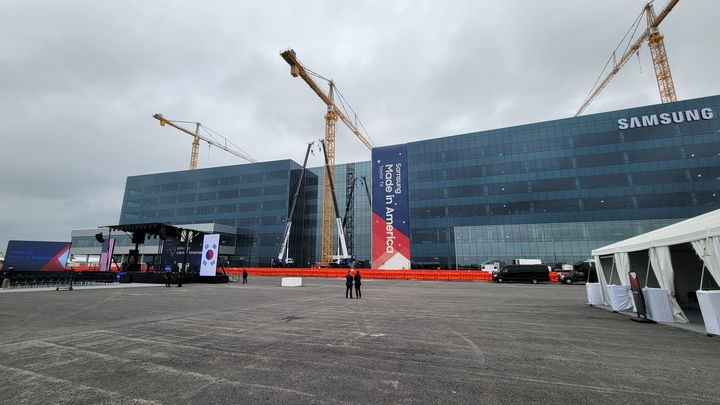
Samsung is now capitalizing on the supply chain challenges, with its Taylor, Texas fabrication plant scheduled to begin operations in the second half of this year.
“Foundry bottlenecks have become severe as demand surges,” an industry official stated. “Samsung is exploring ways to operate its facilities more flexibly to capture this increased demand.”
As part of this strategy, Samsung is accelerating its plans for a “hybrid” semiconductor production system, enabling it to switch between advanced logic chips and next-generation memory.
Construction of the P5 complex at its Pyeongtaek campus in Gyeonggi Province is proceeding faster than anticipated. This facility – designed as Samsung’s first “triple fab” featuring three floors and up to 12 cleanrooms – is increasingly expected to support both memory and foundry production, although final line allocation is yet to be determined.
This enhanced flexibility could allow Samsung to respond more rapidly to shifts in market demand, particularly as AI-driven workloads increasingly blur the distinctions between memory and logic chips.
However, analysts caution that realizing this opportunity depends on execution.
“The key question is whether Samsung can convert current supply limitations into sustainable customer growth, rather than just a temporary increase,” an industry official commented.