SK hynix Advances AI Memory Production with Groundbreaking U.S. Semiconductor Facility in Indiana
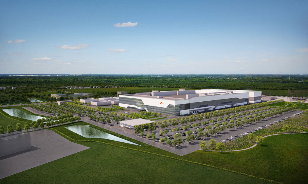
SK hynix has initiated construction on its first semiconductor manufacturing facility in the United States, marking a pivotal expansion of its advanced packaging capacity specifically designed for artificial intelligence (AI) memory. This strategic investment aims to significantly bolster SK hynix’s global supply chain and address the escalating demand for high-performance AI chips.
According to recent reports from Herald Business, the global semiconductor giant commenced foundational piling work at its Indiana site. This crucial step signifies the official start of construction for a cutting-edge advanced packaging plant dedicated to AI applications. Groundwork is anticipated to continue for several months, with above-ground construction projected to begin in the latter half of the year.
This ambitious project is backed by SK hynix’s 2024 commitment to invest $3.87 billion into the expansive 56-hectare facility. The Indiana plant is slated to achieve mass production by the second half of 2028, focusing on the fabrication of next-generation high bandwidth memory (HBM) products, including advanced HBM4E and HBM5 chips.
The establishment of the Indiana facility is a cornerstone of SK hynix’s broader vision to create a robust global AI memory ecosystem. This network will seamlessly integrate its key domestic production hubs in Yongin and Icheon (Gyeonggi Province), along with Cheongju (North Chungcheong Province), with its strategic U.S. operations. Additionally, the plant’s proximity to Purdue University is expected to foster valuable collaborations with leading local research institutions, accelerating innovation in advanced semiconductor technologies.
In the rapidly evolving AI era, advanced packaging has emerged as an indispensable technology. It directly impacts the performance, efficiency, and yield of vertically stacked HBM chips, which are essential components for high-performance computing and complex AI workloads.
Complementing its U.S. expansion, SK hynix is also accelerating its domestic investments. The company is actively building a substantial 19 trillion won ($12.9 billion) advanced packaging facility in Cheongju, projected for completion by 2027. Furthermore, SK hynix is expanding its DRAM capacity at the M15X fab, where a second clean room began operating ahead of schedule in March, further solidifying its manufacturing capabilities.
To ensure technological leadership, SK hynix plans to deploy approximately 20 state-of-the-art extreme ultraviolet (EUV) systems from ASML across its key production lines. These advanced systems will support the development and manufacturing of next-generation DRAM processes.
Despite these significant investments and strategic advancements, industry experts anticipate that semiconductor supply constraints may persist. Chey Tae-won recently cautioned that potential shortages in critical resources could limit global memory output through 2030, highlighting ongoing challenges in the semiconductor supply chain.
Nevertheless, SK hynix continues to demonstrate strong financial performance, with analysts forecasting another record quarter. Operating profits are projected to reach an impressive 40 trillion won, underscoring the company’s robust market position and effective growth strategies.
jylee